
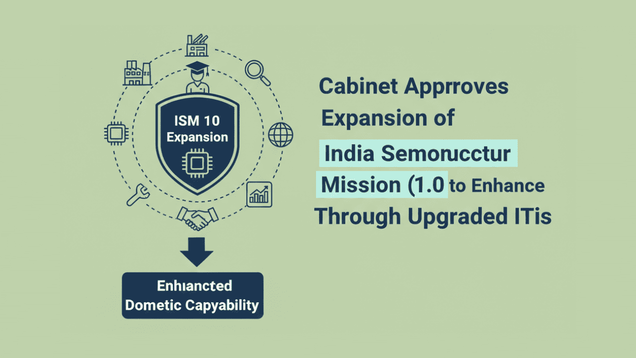
NEW DELHI – In a move destined to redefine India’s position in the global technology value chain, the Union Cabinet has officially approved the strategic expansion of the India Semiconductor Mission (ISM) 1.0 and launched the ambitious ISM 2.0. This transition marks a decisive shift from merely attracting assembly and testing operations to building a comprehensive, full-stack semiconductor ecosystem on Indian soil. Announced during the Union Budget 2026-27, the mission receives an immediate financial push and a recalibrated policy framework designed to achieve technological sovereignty. The Prime Minister’s vision for this expansion is clear: India will no longer just be a consumer of electronics but a primary creator of the foundational components that power the modern world.
As the global landscape shifts toward “technological nationalism” and supply chain fragmentation, the expansion of ISM represents India’s proactive response to secure its digital future. The semiconductor sector, which underpins everything from 5G infrastructure and AI to automotive electronics and defense systems, is the new frontier of national security. By doubling down on the successes of ISM 1.0, the government is ensuring that the momentum generated by early fabrication projects in states like Gujarat and Maharashtra is not only sustained but accelerated toward the goal of a $110 billion domestic semiconductor market by 2030.
The Success Story of ISM 1.0: Building the Foundation
Before delving into the future, it is essential to acknowledge the groundwork laid by the initial phase of the mission. Launched in December 2021 with a ₹76,000 crore incentive framework, ISM 1.0 was the first serious attempt at building a silicon ecosystem in India. As of early 2026, the results are tangible. Ten major semiconductor projects have already been approved, representing a cumulative investment of approximately ₹1.60 lakh crore across six states.
These projects include India’s first private semiconductor fabrication plant (Fab) by Tata Electronics in Dholera, Gujarat, and advanced packaging facilities that have already begun pilot production. This phase successfully demonstrated that India could attract global giants and homegrown conglomerates alike to invest in high-tech manufacturing. However, ISM 1.0 was primarily focused on “downstream” activities—assembly, testing, and basic packaging (ATMP/OSAT). The expansion now approved by the Cabinet seeks to move “upstream” into the more complex and high-value layers of the semiconductor value chain.
Launching ISM 2.0: Deepening the Ecosystem
The newly approved ISM 2.0 is the centerpiece of the Cabinet’s decision. Unlike its predecessor, which focused on creating an ecosystem, ISM 2.0 focuses on deepening it. The mission has been allocated an additional ₹1,000 crore for the fiscal year 2026-27 specifically to target three critical pillars: Equipment and Materials, Design Intellectual Property (IP), and R&D Centers.
One of the most significant bottlenecks in the semiconductor industry is the reliance on foreign-made equipment and raw materials. Currently, India imports nearly 100% of its specialized semiconductor manufacturing equipment. ISM 2.0 introduces a dedicated scheme to incentivize the domestic production of precision tooling, chemicals, and gases required for chip making. By localizing the supply of capital goods, the government aims to lower the high capital expenditure (CAPEX) usually associated with setting up chip factories. This “backward integration” is what will make the Indian semiconductor industry truly self-reliant and resilient to global supply disruptions.
Driving Indigenous Innovation through Chip Design and IP
The second major focus of the expansion is the creation of “Full-Stack Indian IP.” While India has long been a hub for semiconductor design services, most of the intellectual property generated belongs to multinational corporations. ISM 2.0 seeks to change this by supporting domestic startups and academic institutions in developing homegrown processor architectures.
The government highlighted the success of the Design Linked Incentive (DLI) Scheme, which already supports 24 semiconductor design startups. These firms have successfully attracted venture capital and are now working on advanced foundry nodes, including 12nm technology. With the new expansion, the Cabinet has set a roadmap to achieve the capability to design and manufacture chips at the 3nm and 2nm nodes by the next decade. The launch of the DHRUV64, a fully indigenous 64-bit microprocessor, serves as a prime example of the “Made in India” IP that the government intends to scale across 5G, automotive, and IoT sectors.
Expansion of the Electronics Components Manufacturing Scheme (ECMS)
To complement the chip-making push, the Cabinet has also approved a massive increase in the outlay for the Electronics Components Manufacturing Scheme (ECMS). Originally launched in April 2025 with an outlay of roughly ₹23,000 crore, the scheme’s budget has been raised to ₹40,000 crore due to overwhelming industry response.
This expansion targets the high-value components that make up 60-70% of the value of smartphones and laptops, such as display modules, camera assemblies, and Printed Circuit Boards (PCBs). By co-locating component manufacturing with semiconductor fabs, the government is creating a “circular manufacturing” environment. This reduces lead times, lowers costs, and ensures that India captures a larger share of the value in the electronics sector, rather than just acting as a final assembly point.
Talent Development and Industry-Led Research
A developed semiconductor ecosystem requires a highly specialized workforce. Recognizing this, the Cabinet has approved the establishment of industry-led research and training centers. These centers will be partnered with central public sector enterprises and top academic institutions to bridge the talent gap. Over 67,000 students are already being trained in VLSI (Very Large Scale Integration) design and integrated circuit manufacturing under programs facilitated by the AICTE and NIELIT.
The goal is to create a pipeline of “fab-ready” engineers and technicians. These training centers will focus on hands-on experience with industry-grade EDA (Electronic Design Automation) tools, ensuring that the human capital is ready to operate the multi-billion dollar fabrication units as they come online. The government’s decision to modernize the Semiconductor Laboratory (SCL) in Mohali with a ₹4,500 crore investment further underscores the commitment to keeping R&D at the heart of the mission.
Conclusion: A Strategic Leap Toward Technological Sovereignty
The Cabinet’s approval of the expansion of ISM 1.0 and the launch of ISM 2.0 represents a strategic reset of India’s technological ambitions. By addressing the weakest links in the value chain—equipment, materials, and IP—the government is ensuring that India’s growth is not dependent on foreign permissions or external supply chains. This “Infra-First” and “IP-First” strategy positions India not as a low-cost substitute for other manufacturing hubs, but as a primary, strategic partner in the global tech economy.
As these schemes move from policy to execution, the impact will be felt across every sector of the economy. From creating high-quality employment for thousands of young engineers to reducing the trade deficit in electronics, the expanded India Semiconductor Mission is the foundation upon which the Viksit Bharat of 2047 will be built. The “Sovereign Chip” is no longer a distant dream; it is a rapidly maturing reality.